

STS Software Development
Wir unterstützen Sie während Ihres gesamten Wertschöpfungsprozesses, von der Entwicklung bis zum Vertrieb.

Unsere Philosophie
STS Software Development betreut Sie auf verantwortungsvolle Art und Weise in allen Fragen zu Ihren geschäftlichen Abläufen – von Entwicklung bis Vertrieb.

Unsere Leistungen
Anforderungsanalyse, Erarbeitung eines Lösungskonzepts, Schulungen der Anwender, Betreuung der Kunden und vieles mehr.

Unser Versprechen
Wir optimieren Ihren Entwicklungsprozess und stellen unser über viele Jahre gewachsenes Know-How und Fachwissen zur Verfügung.
Software-Entwicklung mit STS
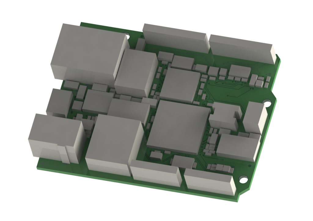
Die Leiterplattenentwicklung erreicht ein neues Level: In immer mehr Bereichen ist die Leiterplatte ein unverzichtbares Element.
Ein detaillierter Lagenaufbau und die Erfüllung verschiedenster mechanischer Voraussetzungen in Kombination mit elektronischen Faktoren sind dabei unerlässlich für den Erfolg Ihres Produkts.
Unterstützung von Entwicklung bis Vertrieb
Wir unterstützen Sie während Ihres gesamten Wertschöpfungsprozesses, von der Entwicklung bis zum Vertrieb.
Unser aufeinander abgestimmtes Produkt-Portfolio beinhaltet ausgewählte Import-/Export-Funktionen und bietet Ihnen somit eine ausgezeichnete Plattform der für Sie relevanten Software.